SHENZHEN, China, Jan. 24, 2025 -- In the design of wearable devices, every millimeter matters. As AI technology becomes deeply integrated, wearable devices demand not only enhanced performance but also the ability to deliver more functionalities within highly limited spaces. Recently, Longsys(301308.SZ) introduced a 7.2mm × 7.2mm subsize eMMC, providing a groundbreaking memory solution for optimizing the physical space of AI wearables.
Ultra-Compact: Unlocking New Possibilities for Wearable Design
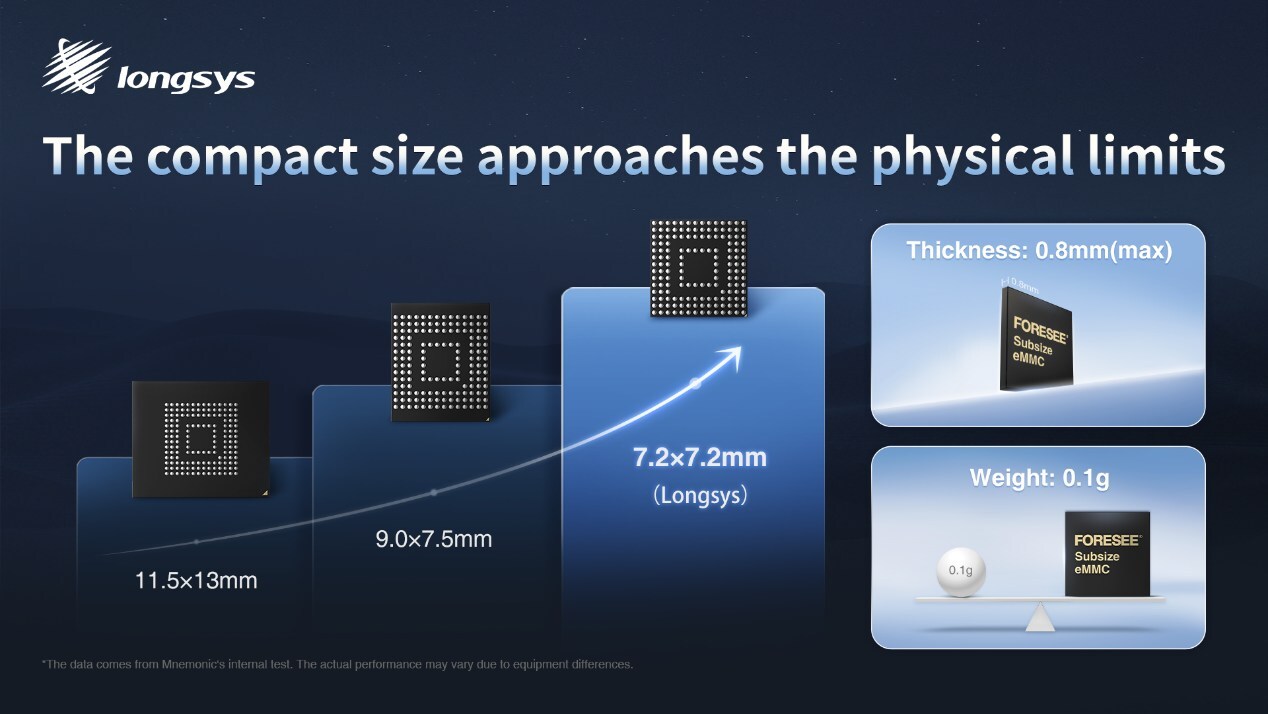
7.2mm × 7.2mm is one of the smallest subsize eMMCs currently available on the market, achieving maximum space efficiency. Its 153 solder balls nearly cover the entire panel, pushing the design to the very edge of physical limits. Compared to the standard 11.5mm × 13mm eMMC, its surface area is reduced by approximately 65%, with a thickness of just 0.8mm. Featuring a lightweight design, it weighs only 0.1g (approx.), nearly 67% lighter than the standard 0.3g eMMC. This ultra-compact design frees up additional space for other internal components, enabling wearable devices to maintain a sleek and lightweight form while integrating more functional modules to meet diverse user demands.
Compact Yet Capable: Balancing Capacity and Performance
While pursuing an ultra-compact design, the 7.2mm × 7.2mm subsize eMMC does not compromise on performance or capacity. Equipped with in-house firmware, it ensures fast device boot-up, seamless AI application performance, and efficient data processing. Additionally, low-power technologies, such as intelligent sleep and dynamic frequency scaling, significantly reduce energy consumption and extend battery life without compromising performance. With capacities of 64GB and 128GB—among the highest for similar compact products—it offers innovative solutions for optimizing AI wearables such as smart glasses, watches, and earphones.
In-House Packaging and Testing: Leading the Industry
Notably, this subsize eMMC is packaged and tested at Longsys' in-house Suzhou Packaging & Testing Base, and it adopts an innovative grinding and cutting process to achieve a smaller size. The facility specializes in NAND Flash and DRAM packaging and testing while extending its capabilities to eMMC, UFS, eMCP, and ePOP series, offering comprehensive services across wafer-level, chip-level, and system-level packaging.
PTM Full-Stack Customization: Beyond Compactness
Advanced packaging technologies give Longsys a competitive edge in product size, thermal management, compatibility, reliability, and storage capacity. Longsys' eMMC products are now highly mature, with 2024 seeing the launch of its proprietary eMMC controllers and QLC eMMC. Beyond compact design, its full-stack customization capabilities extend across product development, technology, and manufacturing to meet diverse client needs.
The launch of the 7.2mm × 7.2mm ultra-compact eMMC represents a new breakthrough for mature products, offering robust support and enhanced options for AI wearable development. Looking ahead, Longsys remains committed to memory technology innovation, bringing more exciting possibilities to wearable devices.
About Longsys
Founded in 1999, Longsys(301308.SZ) is a globally leading branded semiconductor memory enterprise, integrating R&D, design, packaging and testing, manufacturing, and sales services. Longsys upholds the corporate vision of "Everything for memory." With memory technology innovation at its core, Longsys provides high-end, flexible, and efficient full-stack customized services to global customers. For more information please visit https://www.longsys.com/, and follow Longsys on LinkedIn, Facebook and Twitter.
This News is brought to you by Qube Mark, your trusted source for the latest updates and insights in marketing technology. Stay tuned for more groundbreaking innovations in the world of technology.


