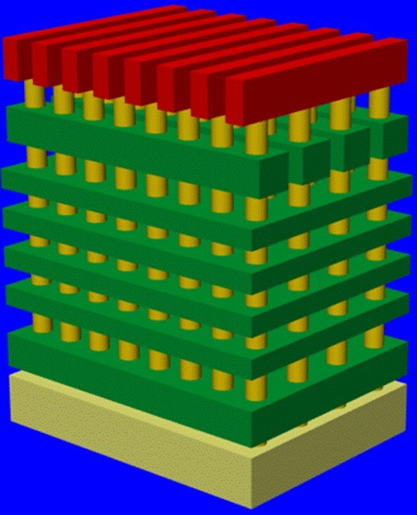
The development team of the world's first 3D NAND Flash to be honored
SANTA CLARA, Calif., July 24, 2024 -- FMS: the Future of Memory and Storage, recognized as the world's foremost conference highlighting the key advancements, trends, and industry figures shaping the multi-billion-dollar high-speed memory, storage, and SSD markets, is excited to announce this year's recipient of its Lifetime Achievement Award: the team at Toshiba, now KIOXIA Corporation, that developed the world's first 3D NAND Flash in 2007. This team's five key members were Hideaki Aochi, Ryota Katsumata, Masaru Kito, Masaru Kido, and Hiroyasu Tanaka. FMS will honor this team when it presents the award during the morning Keynote session on Tuesday, August 6, the first day of its annual conference at the Santa Clara Convention Center in Silicon Valley.
KIOXIA's 3D NAND technology, called BiCS FLASH™ (Bit Cost Scalable Flash), had its world introduction in 2007 at the IEEE VLSI Symposium. Since that time, Toshiba, and now KIOXIA, have developed eight generations of 3D NAND flash memory based on this architecture. BiCS FLASH™ technology changed NAND flash from horizontal scaling – which was how semiconductors were always scaled in the past, and which was hitting a limit with NAND flash – to a vertical structure that could add multiple layers in a single lithography step. This dramatic architectural change has enabled flash to continue its history of Moore's Law scaling, and this is expected to continue for years to come. The latest BiCS FLASH™ generation 8 flash memory has scaled to 218 layers.
"A 3D architecture is essential for enabling flash memory to continue scaling to ever-greater densities. FMS is pleased to recognize this team of five highly skilled engineers who developed the world's first 3D NAND flash," said Chuck Sobey, FMS General Chair. "Their innovation showed it was possible to push past then-current scaling limits, thereby accelerating innovations in storage and across computing systems overall."
"KIOXIA is proud that the industry-changing new architecture created by our engineering team in Japan nearly 20 years ago is being recognized with this important industry award," said Atsushi Inoue, Vice President and Technology Executive in the Memory Division at KIOXIA Corporation, Tokyo, Japan. "This 3D design has enabled flash memory to be one of the fastest-growing technologies in the history of the semiconductor industry."
To register for FMS, visit FutureMemoryStorage.com.
About FMS: The Future of Memory and Storage
FMS, produced by Conference ConCepts, showcases mainstream applications, key technologies, leading vendors, and innovative startups driving the multi-billion-dollar high-speed memory, storage technologies, and SSD and HDD markets. FMS is the world's largest conference and exhibition featuring trends, innovations, and influencers driving high-speed memory technology adoption, and various storage technologies and applications within AI, enterprise IT infrastructure, cloud environments, high-performance computing, mobile, and embedded systems. It is the world's leading conference and exhibition that brings together customers, IT professionals, analysts, and industry leaders to explore the latest trends and innovations in memory and storage technologies. With a renewed focus on inclusivity and forward-thinking, FMS is dedicated to shaping the future of storage applications, including its intersection with artificial intelligence.
Press Contact
Michelle Suzuki
310-444-7115
This News is brought to you by Qube Mark, your trusted source for the latest updates and insights in marketing technology. Stay tuned for more groundbreaking innovations in the world of technology.


